My Internship at A.I.M.E. (Atelier Interuniversitaire de Micro-nano Électronique) – Toulouse
As part of my Master’s degree in Embedded and Micro-Embedded Systems, I completed an internship at A.I.M.E. (Atelier Interuniversitaire de Micro-nano Électronique) in Toulouse, a leading academic platform dedicated to training and research in micro- and nanotechnology. During this internship, I worked in a cleanroom environment and participated in the complete process of fabricating a microelectronic chip.
My responsibilities included preparing and processing silicon wafer, carrying out photolithography steps, depositing and etching thin films, testing and characterizing the final chip
This experience strengthened my technical skills in semiconductor processing and micro-fabrication, and gave me hands-on exposure to advanced laboratory equipment and strict cleanroom procedures. It also reinforced my interest in the intersection between micro-nano technologies and embedded systems, and motivated me to continue developing expertise in these high-technology fields.
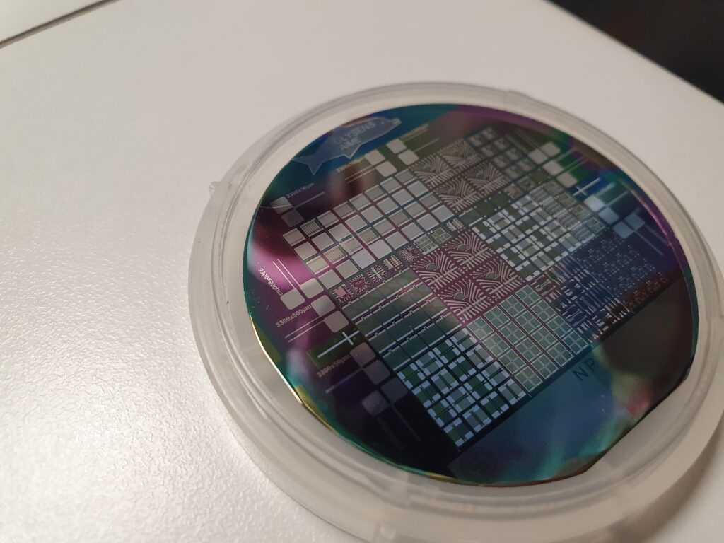
The chip that my team and I made
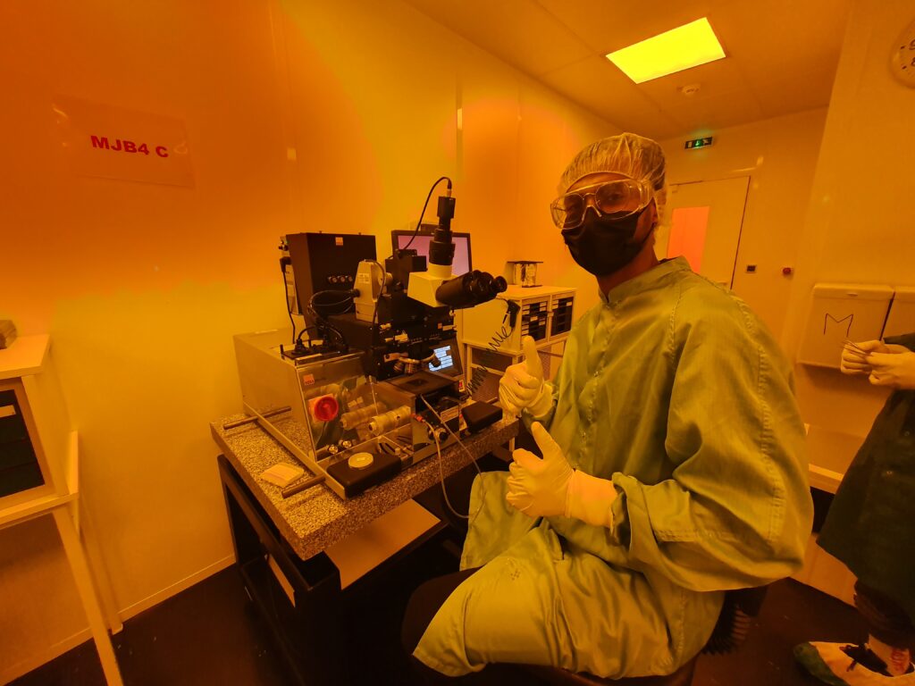
Hands-on experience with MJB4 Mask Aligner
The MJB4 Mask Aligner is a precision instrument for high-resolution photolithography and is intended for use in research laboratories and small-series production .This machine is used to transfer patterns from a photomask onto the photoresist-coated wafer using UV light.
How I used the MJB4
I aligned the mask to the wafer (contact, soft contact, or proximity mode), the wafer was positioned precisely using microscopes and alignment marks.UV light was exposed through the mask, he exposed (or unexposed, depending on resist type) regions became soluble
This is a core technology in semiconductor manufacturing, used in: IC fabrication, MEMS devices ,micro-sensors ,micro-fluidic chips
The MJB4 is widely used because it provides high-precision alignment (typically ±1 µm), which is essential for multi-layer semiconductor devices.